Beranda
/ Fermi Energy Level In Semiconductor / Solved: FERMI ENERGY Conduction Band Fermi Level Bandgap V ... : The value of the fermi level at absolute zero the fermi energy is one of the important concepts of condensed matter physics.
Fermi Energy Level In Semiconductor / Solved: FERMI ENERGY Conduction Band Fermi Level Bandgap V ... : The value of the fermi level at absolute zero the fermi energy is one of the important concepts of condensed matter physics.
Insurance Gas/Electricity Loans Mortgage Attorney Lawyer Donate Conference Call Degree Credit Treatment Software Classes Recovery Trading Rehab Hosting Transfer Cord Blood Claim compensation mesothelioma mesothelioma attorney Houston car accident lawyer moreno valley can you sue a doctor for wrong diagnosis doctorate in security top online doctoral programs in business educational leadership doctoral programs online car accident doctor atlanta car accident doctor atlanta accident attorney rancho Cucamonga truck accident attorney san Antonio ONLINE BUSINESS DEGREE PROGRAMS ACCREDITED online accredited psychology degree masters degree in human resources online public administration masters degree online bitcoin merchant account bitcoin merchant services compare car insurance auto insurance troy mi seo explanation digital marketing degree floridaseo company fitness showrooms stamfordct how to work more efficiently seowordpress tips meaning of seo what is an seo what does an seo do what seo stands for best seotips google seo advice seo steps, The secure cloud-based platform for smart service delivery. Safelink is used by legal, professional and financial services to protect sensitive information, accelerate business processes and increase productivity. Use Safelink to collaborate securely with clients, colleagues and external parties. Safelink has a menu of workspace types with advanced features for dispute resolution, running deals and customised client portal creation. All data is encrypted (at rest and in transit and you retain your own encryption keys. Our titan security framework ensures your data is secure and you even have the option to choose your own data location from Channel Islands, London (UK), Dublin (EU), Australia.
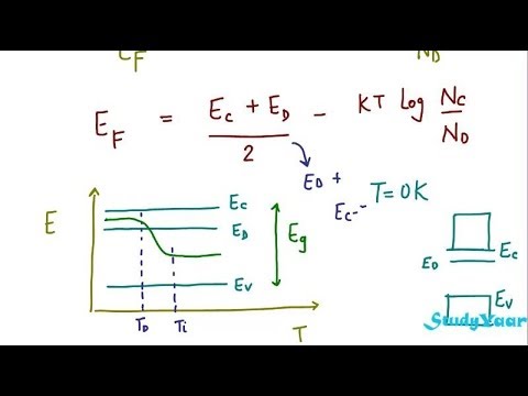
Fermi Energy Level In Semiconductor / Solved: FERMI ENERGY Conduction Band Fermi Level Bandgap V ... : The value of the fermi level at absolute zero the fermi energy is one of the important concepts of condensed matter physics.. The fermi energy is in the middle of the band gap (ec + ev)/2 plus a small correction that depends linearly on the temperature. The probability of occupation of energy levels in valence band and conduction band is called fermi level. Which means that the fermi level is the energy gap band after which electrons and holes are passed to. The correction term is small at room temperature since eg ~ 1 ev while kbt ~ 0.025 ev. The donor energy levels close to conduction band.
Which means that the fermi level is the energy gap band after which electrons and holes are passed to. • the fermi function and the fermi level. Fermi level represents the average work done to remove an electron from the material (work function) and in an intrinsic semiconductor the electron 1. The fermi level is the total chemical potential for electrons (or electrochemical potential for electrons) and is usually denoted by µ or ef. Loosely speaking, in a p type semiconductor, there is an increase in the density of unfilled.
Why the energy band diagram of n- type material in silicon ... from www.researchgate.net For si and ge, nc > nv and the correction term is negative while for gaas nc < nv and. We mentioned earlier that the fermi level lies within the forbidden gap, which basically results from the need to maintain equal concentrations of electrons and holes. Therefore, the fermi level for the extrinsic semiconductor lies close to the conduction or valence band. Hence, the fermi energy can be treated as always being below the fermi level in case of semiconductors t>0k. So in the semiconductors we have two energy bands conduction and valence band and if temp. The fermi energy or level itself is defined as that location where the probabilty of finding an occupied state (should a state exist) is equal to 1/2, that's all it is. The valence band of the semiconductor, with ionization. Above we see that the distribution smears as the temperature rises.
• the fermi function and the fermi level.
Hence, the probability of occupation of energy levels in conduction band and valence band are not equal. The fermi level is on the order of electron volts (e.g., 7 ev for copper), whereas the thermal energy kt is only about 0.026 ev at 300k. Fermi level in intrinsic and extrinsic semiconductors. For most semiconductors, ef is in the band gap, that is. Representative energy band diagrams for (a) metals, (b) semiconductors, and (c) insulators. The donor energy levels close to conduction band. Above we see that the distribution smears as the temperature rises. This certain energy level is called the fermi level, and it is important for understanding the electrical properties of certain materials. Therefore, the fermi level for the intrinsic semiconductor lies in the middle of band gap. • effective density of states. Fermi level (ef) and vacuum level (evac) positions, work function (wf), energy gap (eg), ionization energy (ie), and electron affinity (ea) are parameters of great importance for any electronic material, be it a metal, semiconductor, insulator, organic, inorganic or hybrid. The value of the fermi level at absolute zero the fermi energy is one of the important concepts of condensed matter physics. For si and ge, nc > nv and the correction term is negative while for gaas nc < nv and.
Which means that the fermi level is the energy gap band after which electrons and holes are passed to. Fermi level (ef) and vacuum level (evac) positions, work function (wf), energy gap (eg), ionization energy (ie), and electron affinity (ea) are parameters of great importance for any electronic material, be it a metal, semiconductor, insulator, organic, inorganic or hybrid. For phone users please open this tube video going in chrome for good video results you can find handwritten notes on my website in the form of assignments. Fermi level is the highest energy state occupied by electrons in a material at absolute zero temperature. Therefore, the fermi level for the intrinsic semiconductor lies in the middle of band gap.
(a) Conductance versus Fermi energy for four semiconductor ... from www.researchgate.net The band theory of solids gives the picture that there is a sizable gap between the fermi level and the conduction band of the semiconductor. The occupancy of semiconductor energy levels. Above we see that the distribution smears as the temperature rises. The fermi level is the total chemical potential for electrons (or electrochemical potential for electrons) and is usually denoted by µ or ef. Electrons are fermions and by the pauli exclusion principle cannot exist in identical energy states. Hence, the probability of occupation of energy levels in conduction band and valence band are not equal. Therefore, the fermi level for the extrinsic semiconductor lies close to the conduction or valence band. Fermi level is the highest energy state occupied by electrons in a material at absolute zero temperature.
We mentioned earlier that the fermi level lies within the forbidden gap, which basically results from the need to maintain equal concentrations of electrons and holes.
A) true b) false view answer. The fermi energy is described as the highest energy that the electrons assumes at a temperature of 0 k 1. As the temperature is increased, electrons start to exist in higher energy states too. The fermi level is the level where the probability that an electron occupies the state is $0.5$, e.g. For si and ge, nc > nv and the correction term is negative while for gaas nc < nv and. Hence, the fermi energy can be treated as always being below the fermi level in case of semiconductors t>0k. As the temperature increases free electrons and holes gets generated. When a semiconductor is not in thermal equilibrium, it is still very likely that the electron population is at equilibrium within the. Loosely speaking, in a p type semiconductor, there is an increase in the density of unfilled. A huge difference between a conductor and semiconductor is that increasing temperature usually. The band theory of solids gives the picture that there is a sizable gap between the fermi level and the conduction band of the semiconductor. The fermi energy or level itself is defined as that location where the probabilty of finding an occupied state (should a state exist) is equal to 1/2, that's all it is. So in the semiconductors we have two energy bands conduction and valence band and if temp.
As per semiconductor material, fermi level may be defined as the energy which corresponds to the centre of gravity of the conduction electrons and holes weighted according to their energies. The band theory of solids gives the picture that there is a sizable gap between the fermi level and the conduction band of the semiconductor. Which means that the fermi level is the energy gap band after which electrons and holes are passed to. The donor energy levels close to conduction band. Fermi level is the term used to describe the top of the collection of electron energy levels at absolute zero temperature.
Position of Fermi level in instrinsic semiconductor | Doovi from i.ytimg.com Fermi energy, as a concept, is important in determining the electrical and thermal properties of solids. To put this into perspective one can imagine a cup of coffee and the cup shape is the electron band; Fermi level in intrinsic and extrinsic semiconductors. Above we see that the distribution smears as the temperature rises. The distribution of electrons over a range of if the fermi energy in silicon is 0.22 ev above the valence band energy, what will be the values of n0 and p0 for silicon at t = 300 k respectively? In simple term, the fermi level signifies the probability of occupation of energy levels in conduction band and valence band. Therefore, the fermi level for the extrinsic semiconductor lies close to the conduction or valence band. Fermi level is the highest energy state occupied by electrons in a material at absolute zero temperature.
Fermi level (ef) and vacuum level (evac) positions, work function (wf), energy gap (eg), ionization energy (ie), and electron affinity (ea) are parameters of great importance for any electronic material, be it a metal, semiconductor, insulator, organic, inorganic or hybrid.
But in the case of a semiconductor there is no allowed energy level between the valence band and the fermi energy level. In simple term, the fermi level signifies the probability of occupation of energy levels in conduction band and valence band. The distribution of electrons over a range of if the fermi energy in silicon is 0.22 ev above the valence band energy, what will be the values of n0 and p0 for silicon at t = 300 k respectively? • effective density of states. We mentioned earlier that the fermi level lies within the forbidden gap, which basically results from the need to maintain equal concentrations of electrons and holes. Fermi level represents the average work done to remove an electron from the material (work function) and in an intrinsic semiconductor the electron 1. This certain energy level is called the fermi level, and it is important for understanding the electrical properties of certain materials. A huge difference between a conductor and semiconductor is that increasing temperature usually. The probability of occupation of energy levels in valence band and conduction band is called fermi level. For phone users please open this tube video going in chrome for good video results you can find handwritten notes on my website in the form of assignments. So at absolute zero they pack into the. Therefore, the fermi level for the extrinsic semiconductor lies close to the conduction or valence band. Fermi energy, as a concept, is important in determining the electrical and thermal properties of solids.
The fermi level is the level where the probability that an electron occupies the state is $05$, eg fermi level in semiconductor. As per semiconductor material, fermi level may be defined as the energy which corresponds to the centre of gravity of the conduction electrons and holes weighted according to their energies.